Emad Najafidehaghani
Emad Najafidehaghani is preparing gold on silicon for the purpose of Kelvin probe microscopy. He transfers molybdenum disulfide on top of the gold. Because of the difference between the work functions of gold and molybdenum disulfide it is possible to see the difference in work function with Kelvin probe microscopy technique with the help of his colleague he was able to to fabricate this substrate in the clean room as following, Using a 4-inch silicon WaferSpotting titanium and gold on top of the silicon wafer which gives a better adhesion to the silicon then by spin coating a PMMA layer, it is possible two dice the same sample with a special machine and later on before transferring molybdenum disulfide he should remove the PMMA in acetone. You can also use different materials such as aluminium to study the work function of molybdenum disulfide please note that this technique works for understanding the difference between the work function of the 2D material and the gold or aluminium and if the work function of the aluminium is known you can can calculate the work function of molybdenum disulfide accordingly.
Emad Najafidehaghani has made tungsten disulfide devices with the help of e-beam lithography with the help of his colleague in the clean room. The electrode pads are far from the active area of the devices, the reason is that measurement probes are very close to the active area and to capture the the electroluminescence of the devices he needs to focus his objectives very close to the device. One disadvantage of long pads is that they bring leakages through the oxide, the longer and more surface area and electrode has the more leakage the device will have through the oxide. in this case he has used back gate oxide, which is basically on top of a heavily doped silicon that means the whole backside of the chip can be by used as a gate electrode. In the inset you can see that the probe is touched the electrode. Tungsten disulfide can be used as a electroluminescent device and as a photodetector in the form of Monolayer.
Emad Najafidehaghani Is explaining about Mean free path of molecules inside ultrahigh vacuum chamber. The vacuum chamber can reach the vacuum of around 10 ^ -10 millibar this means that if two molecules want to collide to eachother, they need to to travel 40 km to be able to have the collision. Th ultrahigh vacuum is needed for measurements like x-ray photoelectron spectroscopy or scanning tunnelling microscopy especially when you a 2D material is such as MoS2 WS2 MoSe2 WSe2 InSe is going to be investigated .
To be able to have to ultra-high vacuum, one needs to aneal the chamber while pumping the chamber for 2 days. The annealing can be more than 110 degrees Celsius. The windows have to be sealed with aluminium foils because of the difference in the expansion coefficients of metal and Glass Emad Najafidehaghani needs to prepare the chamber for measuring the 2D materials such as MoTe2, MoSe2, MoSSe.
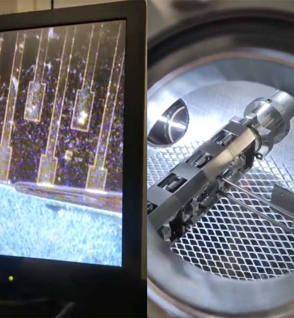
The vacuum probe station is open and I constant flow of Nitrogen Is protecting the samples from the air. Some of the 2D materials are sensitive to the air air4 example MoTe2 or some thin-film organic materials. Emad Najafidehaghani is Trying to put the samples inside in a short time. The probe station has 4 probe arms and one optical arm . The probe Arms are flexible and the probe tips are made of tungsten.
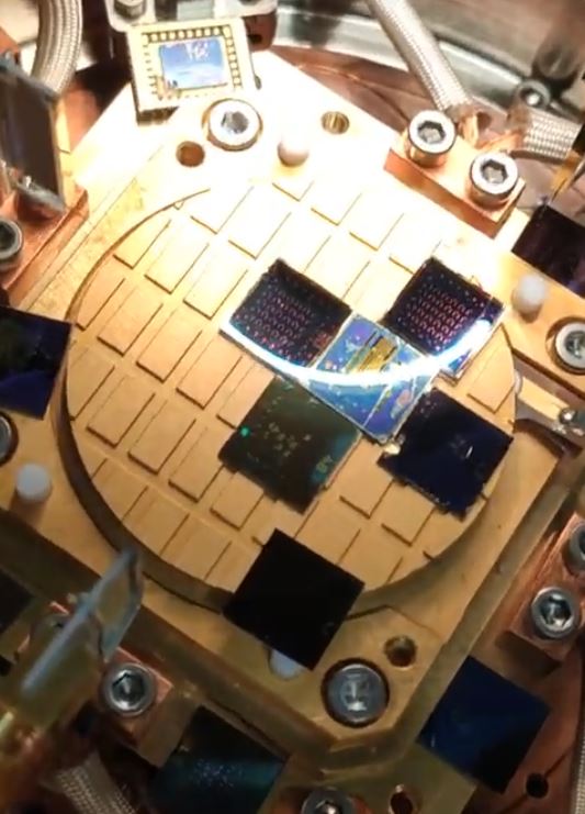
Samples are placed inside a vacuum Probe station The Golden area behind the wafers can be used as a global Gate. Emad Najafidehaghani is placing TMD heterostructures for measuring under high vacuum. The tungsten tips are connected to manual Arms and can be precisely positioned by observing through a high distance objective lens. Transistors and light emitting diodes based on 2D materials such as lateral heterostructure of MoSe2- WSe2 are being measured. As you can see some 2D materials are glued to a chip carrier and to use them, the global back gating is not possible. Lateral heterostructures have applications in the field of optoelectronics.
Low energy electron diffraction Is a technique to measure different parameters in a crystal structure. for example Crystal lattice Constant of grown MoS2 on Au 111 is studied with this equipment. low energy electron diffraction needs ultrahigh vacuum To operate. TMD materials are bombarded with electrons and diffracted towards a fluorescent screen. On the fluorescent screen one can see Brillouin zones and by changing the energy of electrons one can zoom inside the first Brillouin zone.
Measuring Tungsten diselenide under ambient conditions. The equipment has two Hard probes to be able to measure the Micro Devices. the left probe is connected to the source and the right probe is connected to the drain. hard probes can scratch the electrodes on the chip, The WSe2 devices are fabricated on certain triangles with the help of e-beam lithography. The device is on top of silicon dioxide. Silicon dioxide is used as a dielectric and by changing the capacitance between the silicon and tungsten diselenide You can electrostatically bring in or out chargers to the WSe2 layer. This is called gating. Such measurements Under light and air are not accurate, due to the sensitivity of the tmd layer To the light and air molecules. Air molecules change the carrier concentration in the 2d material. Because of the photocurrent generation the resistivity of the layer can be changed. Evaluating the intrinsic properties of tmds in this way is wrong and not accurate unless your device is passivated against air molecules and light.
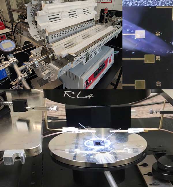
This is a chemical vapour deposition system for growing 2D materials. It has three 3 heating zones, a quartz tube, and vacuum components. The three zones can individually be controlled. Three zones CVD system can be used to grow heterostructures or alloys of TMDs. Emad Najafidehaghani is growing MoSe2 WSe2 to make the thinnest LED based devices. Heterostructures can also be used as photodetectors and rectifiers. MoSe2 is a ntype material (electrons are the majority carriers) and WSe2 is a ptype material (holes are the majority carriers). This combination can bring pn junction structure which is the building blocks in the electronics.
Assembly of a small MOCVD system for deposition of TMD 2D materials, such as monolayer and multilayer WS2. The system is designed to have high controllable pressure and heating.
Atomic force microscopy technique is usually used to check the thickness of TMD materials that we grow such as MoS2, MoSe2 , etc. The AFM can show us different properties of the surface. In normal topography and phase images you can distinguish the difference between materials on the surface, however depending on the methods of the scanning the properties can vary. For example, the phase images of TMDs are more prominent in the contact mode AFM, where we use harder tips to probe the surface. But the contact mode has the possibility of damaging the surface, especially 2D materials. Emad Najafidehaghani mostly tries to do AFM in the tapping mode for MoS2 or other similar TMDs and in special cases, he uses contact mode. Some measurements, for example, KPFM measurements have to be conducted in tapping mode, since the capacitance and deflection of the cantilever is measured in the Kelvin probe force microscopy.
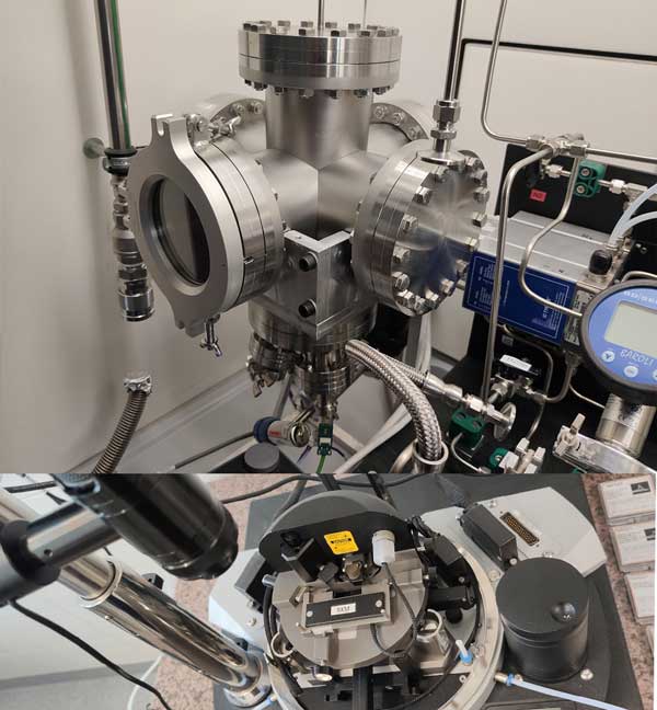
The vacuum cryostat probe station for measuring the electrical and optoelectrical properties of TMDs such as PtSe2, PtS2, MoS2, MoSe2, WSe2, WS2, MoTe2, and more. The objective on the top of the chamber is used to find roughly the position of nano or microdevices. The optical setup on the right side brings the possibility of guiding the laser rays onto the nano or mucro .
devices Inside the chamber. At the bottom, the input for the liquid nitrogen or liquid helium is shown.
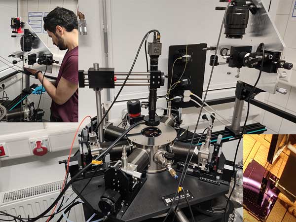
Emad Najafidehaghani is moving the optic stage on a rail to adjust the position of the stage on top of the chamber. The laser diode is installed on top of an in-situ stage. The optoelectrical properties of TMD memtransistors can be studied by such equipments. Memtransistors are devices that can hold the resistance they have on demand. In the literature, it is shown that the memtransistive behavior in 2D materials such as MoS2, comes from the migration of defects in the material, thus changing the Schottky barrier between MoS2 and metal. This means that the migration of defects near the metal junction can influence the measurement current in the device.
The X-Ray photoelectron spectroscopy chamber with an ultrahigh vacuum chamber. The 2D material such as MoS2, WS2 and so on, are grown or transferred on top of the gold. These materials should be on metallic substrates and then substrate should be grounded because after extracting the TMD material electrons They can be charged and if they are connected to metallic grounded substrate, the charging process does not occur. The window is a special .
coated glass beach blocks x Ray from the chamber. The X-ray is generated from the collision of accelerated electrons to an aluminium anode.
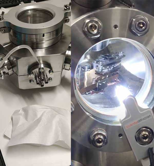
Emad Najafidehaghani Is testing the leakage from the CF connections assembled to the chamber with isopropanol.If the pressure increases this means that the connection is not properly sealed and should be either tightened or the copper gasket should be changed. The connection is a feedthrough for electrical measurements inside the chamber . One can use these 4 feedthrough to measure a transistor and better to say the gas sensor. Source, drain, Gate and ground electrodes can be connected to these ports individually. TMD based gas sensors such as MoS2, PtSe2, MoSe2 , Self assembled monolayers and so on Can be measured inside this chamber.
Low energy electron diffraction technique reveals the Crystal structure parameters by studying the crystal after exposure to the low energy electrons. To study tmd materials such as MoS2 WS2 Nbse2 Crystal structure we can grow these materials on top of Au111. By changing the energy of electrons one can find the first brillouin zone of the crystal structure on top of gold.
By increasing the the energy of electrons the depths of electron penetration increases and one can see the diffraction of electrons from Gold 111 underneath the MoS2 Crystal.
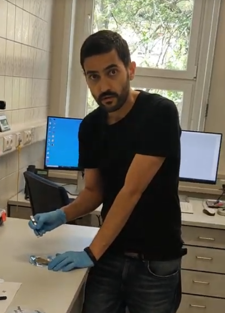
Emad Najafidehaghani is breaking SiO2/Si wafer for the growth of 2D materials such as MoS2, WS2, NbSe2. By pressing a diamond cutter on the Edge of the wafer one can break the crystal into small pieces. You can guide to breaking points using a metallic tweezer on the other side of the wafer, so 2 sides are pressing on the crystal and finally you can have a clean cut on the silicon wafer. The silicon dioxide on top of the silicon has an amorphous structure and is suitable for the growth of tmds. As-grown crystals or suitable for fundamental studies such as PL spectroscopy, XPS UPS, etc. It is not recommended to make electronic devices on top of the as-grown Crystals due to the possible leakage coming from the cracks in the oxide after the growth.
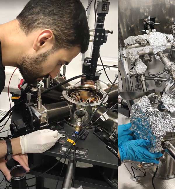
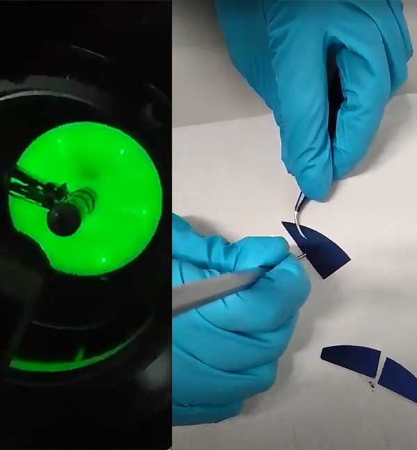
Sometimes after lithography, the electrodes can can be connected to a conductive layer and this brings a large gate leakage current in the measurements and you can not measure the properties of devices accurately, specially in TMDs on thick gate oxides, which sometimes, one needs to work with high back gate voltages (-60 V to 60 V) with materials such as MoS2 or WS2 on 300nm SiO2 gate oxide. To solve this problem, one can gently cut the electrode pad from the conductive layer by a probing tip as shown in the figure. Here it is much better to use flexible probing tips because non flexible tips can damage the oxide. Damaged oxide can cause leakage current from the top electrodes to the back gate electrode.
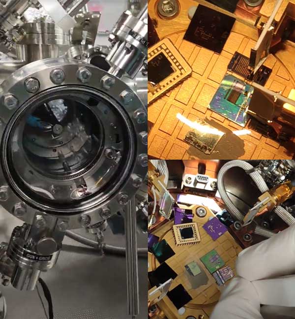
Taking the samples out of the sample holder inside the uhv system. The mesh grid underneath is to prevent the samples from falling into the pumping station. The sample holder is manually rotatable.the samples can be attached on a special carrier, or can be directly used as as-grown materials on SiO2 such as MoS2, WSe2, MoTe2, etc for XPS LEED or UPS measurement .
Responses