Device physics of 2D materials such as MoS2, MoSe2, etc.
Here I will choose MoS2 as an example
-
- Air molecules can have a significant impact on your measurements
- Air molecules can either electrostatically gate the MoS2 layer or there could be a charge transfer happening between the 2D layer and the air molecules
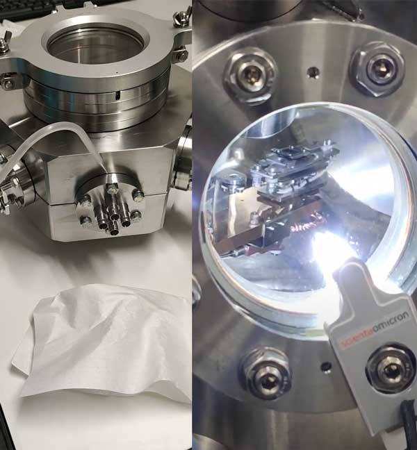
- It is recommended to use Vacuum probes for measuring the intrinsic properties of 2D materials
- The transport mechanism of 2d materials such as MoS2 can change, depending on the measurement temperature conditions. For example, transport can change from band-like transport to hopping transport (for example, this change in the transport mechanism can result in a different electron or hole mobility)
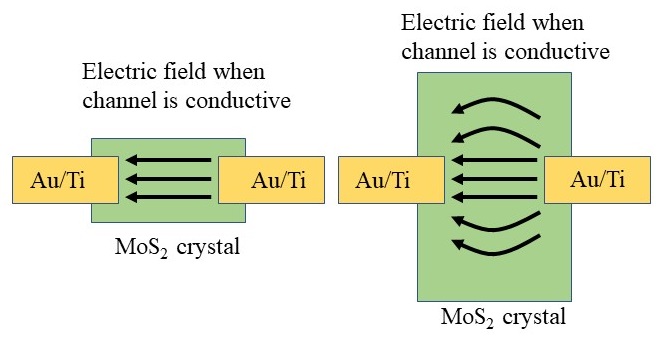
- The structure of the device can significantly change the extracted parameters of the device (electron mobility, threshold voltage, subthreshold swing, photoresponsivity, and …)
- It is recommended to define the channel along with the electrodes because this can create a wrong estimation of the extracted parameters as shown in this figure
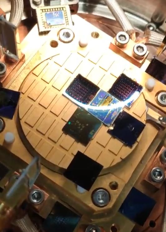
- The area of 2d materials under the contacts is important, due to the direct effect of the charge injection between MoS2 and metal
- The dielectric plays an important role in the behavior of the device. An oxide with high trap states can increase the hysteresis of the device.
- The thinner the oxide (for example less than 100nm), the better the capacitance; but it causes higher leakage current and the risk of breaking the oxide while measurement
- For low-temperature measurements, for example in the case of using Si substrate as a global gate, always use heavily dope silicon, otherwise, it won’t be conductive, since the dopants at low temperatures will take back whatever they gave to the crystal at room temperature! (for example, because the energy levels of the orbitals of phosphor are in the band gap of silicon, at room temperature, their electrons jump into the silicon conduction band, however, at low temperature, the electrons come back to the orbitals and the number of free electrons in the conduction band of silicon will be significantly reduced)
- Choose the electrode metal as per your need. For example, MoS2-Au junction can create an observable Schottky barrier. Here, the Schottky barrier is the difference in the conduction band of MoS2 to the Fermi level of the Au. After the junction between the gold and MoS2, charges (electrons) will be transferred from the MoS2 (with a lower work function) to the Au (with a higher work function). This charge transfer will create an electric field inside the MoS2) which hinders further charge transfer. This electric field bends the conduction and valence band upwards in such a way that the charge transfer is not easy to happen. When you apply an external electric field, you can manipulate this band bending and this can increase the charge injection. This phenomenon is significant in 2D materials because the charges are confined in 2 dimensions and an electric field is forced to be in a confined channel. You can see if the device has a Schottky behavior by doing a simple IV curve measurement. This shows itself in a curved shape. This means at first by increasing the source-drain voltage, the current increases very slowly (nonlinear) and with a further increase in the voltage, the current suddenly increases significantly till it has a linear behavior (if the enhancement of current is extremely high, other effects may play a role).
- If you use metals with similar or lower work functions than MoS2, you can create an ohmic junction. In this case, after the junction, charges transfer from the metal to the MoS2 and the bands bend downwards, making the charges possible to move between the junction in an easy way.
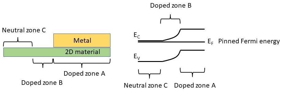
- The 2D material under the metal electrode is differently doped (the charge transfer is not the same!) than the channel. As it its obvious from the Figure, the Fermi energy is pinned to the metal and the Fermi energy level is different depending on the position of the 2D material to the metal.
- Trap states inside the 2D material as well as in the interface and oxide can increase the threshold voltage of the transistor.
- Trap states can decrease the mobility of electrons/holes by interacting with them (deviating the charges), by trapping the charges and detrapping them, or by trapping charges and not getting detrapped (which is most obvious in the low-temperature measurements)
- Some 2D materials can be degraded in the air but it depends on the material, for example, MoS2 is stable in the air even 2 years after the growth from my experience but MoTe2 will be degraded in 1 day! Even some MoS2 devices are still functional after 4 years but with lower yields which are kept in the air.
- The Schottky barrier between the TMDs and the metal is different depending on the defect density of the crystals. For example, more defects in MoS2 create a lower Schottky barrier because of the number of available states in the band gap and more disruption in the electric field by the defects. This means that the created electric field because of the charge transfer from metal to MoS2 can be disturbed by the defects and thus the band bending near the metal-MoS2 can be lower than if there is no defect there.
If you find something which should be corrected. Please let me know.
Our goal is to understand together.
Responses