


Effect of gas molecules on 2D materials
Air molecules can have a significant impact on measurements of 2D materials, particularly when the samples are not protected from the ambient environment. The sensitivity of 2D materials to air molecules can vary depending on the specific material and the measurement technique being used. For example, transition metal dichalcogenides (TMDs) such as MoS2 and WSe2 are particularly sensitive to air molecules because of their van der Waals interactions, which can be easily disrupted by adsorbed contaminants. This can lead to changes in the electronic and optical properties of the material, such as changes in the bandgap and the charge carrier mobility.
On the other hand, graphene is chemically more robust to air molecules because of its strong sp2 hybridization. However, graphene can also be affected by adsorbed contaminants, which can lead to changes in its electronic properties [electrostatic gating or charge transfer].
Encapsulation
In general, the air molecule responsivity of MoS2 can be higher than that of PtSe2 or graphene due to a couple of factors such as van der Waals interactions, defect density, device design, crystallinity, grain boundaries, crystal purity and etc. Therefore, it is important to protect 2D materials samples from the ambient environment when measuring their properties. This can be done by encapsulating the samples in a protective material such as h-BN, or by measuring the samples in a controlled environment, such as a vacuum or inert atmosphere.
Dielectric deposition
Dielectric oxides can also prevent the effect of air molecules on the device channels. When air molecules come into contact with the surface of a 2D material, they can adsorb onto the surface and form a thin layer of contaminants. These contaminants can act as charge donors or acceptors, which can affect the electronic properties of the 2D material. For example, in MoS2 and WSe2, the adsorbed air molecules can act as electron acceptors, which can lead to a reduction in the electron concentration from the TMDs, in other words, an increase in the hole concentration in the material. A decrease in the charge carrier mobility can be a consequence of this process. This is known as the charge transfer effect.
Gating effect
Additionally, air molecules can also act as gate dielectric for 2D materials, for example, the absorbed layer can work as a permanent gating element as well as help non-absorbed molecules to gate the 2D material, which can affect the electronic properties of the material by changing the work function of the material. For example, in MoS2, the adsorbed air molecules [in the case of gating] can change the work function of the material and result in a change in the threshold voltage of the material. This is known as the gating effect.
Charge transfer
It is important to note that the charge transfer and gating effect of air molecules can be different depending on the type of air molecule and the specific 2D material. Therefore, it is important to control the ambient environment when measuring the properties of 2D materials and to use appropriate cleaning methods to remove any adsorbed contaminants from the surface of the material.
Charge scattering
Charge scattering is another side effect of the external molecules on the surface of 2D materials which is a process by which the movement of electrons or holes is impeded or disrupted by the presence of other charged particles or molecules. accumulation of gas molecules at a certain position on the crystal can act as scattering centers for the carriers. This can lead to a reduction in the mobility of the carriers, which can negatively impact the overall conductivity of the material.
Degradation
This is in addition to the fact that air molecules have the possibility of oxidizing the crystal which leads to the degradation of the material quality. In my 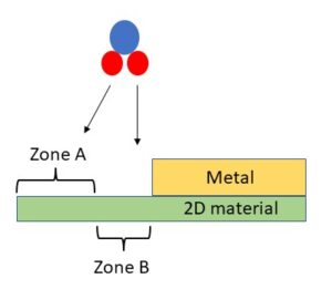 experience, MoS2 is the most stable crystal that I have worked with. For example, I had a couple of grown MoS2 crystals and one chip device 4 years on the shelf under ambient conditions but still works and you can see the MoS2 crystal clearly under an optical microscope, However, in the case of grown MoSe2, the hexagon crystals were degraded after 6 months, but it’s important to mention that triangular shape crystals remained around 1 year.
MoS2 on the shelf
Another important experience for me was the devices that were made on MoSe2 remained for around 2 years, this can show that residual molecules that were used to fabricate the devices may function as an insulation layer for the crystal. Especially, the PMMA transfer technique which is used to transfer the as-grown crystals to the new chip substrate for the fabrication of the MoSe2 devices can provide this insulating possibility.
Effect on contact resistance
It is worthful to mention that the air molecules ca n change the contact resistance of some 2D material devices such as MoS2. This comes from the position of molecule physisorption on zone A or zone B.
In this case of physisorption on zone B the molecule may change the contact resistance of the device. This can be significant due to a couple of factors such as the defect density of MoS2, the position of the grain boundaries, the creation of scattering centers, more electrostatic alteration on the edges (metal-semiconductor junction zone B), more favorable positions for physisorption process and disturbing the charge transfer process after existing additional states in the molecule. This means that the effect of air molecules on contact resistance is highly dependent on the specific device configuration, material quality, and the working environment.
These were my personal experience after measuring 2D material devices such as MoS2 in the air or under vacuum conditions.
Author: Δ Emad Najafidehaghani Δ


