How to measure 2D materials electrically?
I will choose MoS2 as an example
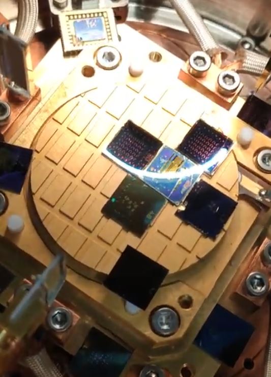
- It’s better to transfer the MoS2 crystals from the growth substrate to another substrate (the reason is due to the probable cracks in some substrates during the growth unless you are sure there is no problem ) (the cracks in the oxide can bring leakage) For example if you grow MoS2 on SiO2 on Si substrate, there is a possibility that the SiO2 have cracks and the cracks cause leakage current
- After transferring the MoS2, be sure that the PMMA is mostly gone by using acetone for at least 1 hour, this is extremely important for making a good metal-semiconductor junction.
- Do not use any ultrasonic during your device fabrication process (the MoS2 can be cracked or damaged-maybe not directly from the substrates but from the nanoparticles that take off from the surface and may hit the surface of the 2D material)
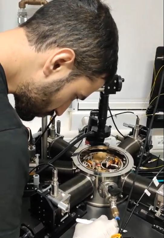
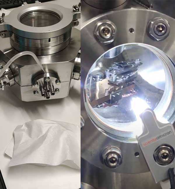
- It is recommended to use flexible probes (like flexible tungsten probes) because there is a possibility of breaking the gate oxides when touching the device
- You can use wire bonding, but it is based on the necessity
- If you use wire bonding, do not design the electrode pads near the 2D channel, because the pressure may damage the crystal, so always the pads should be a little far from the channel
- In 3 channel device (source-drain-gate), connect one of the pads to the source and ground it, connect the other electrode to the drain (this is a variable voltage), and connect the last electrode to the gate (this can be a global back gate, which is the whole substrate, for example heavily doped silicon substrate)(or it can be a top gate depending on your design)
- If the device and the material are unknown to you, fix a gate voltage to 0V and change the drain voltage from 0V to a couple of mV. If you did not see any change in the source-drain current try changing the gate voltage in very small steps from negative to positive voltages. When you are changing the gate voltage, be careful of the current which is measured from your gate, because it shows how much leakage current you have. So if you choose very big gate voltages, you make break the gate oxide. If you still did not see any change in the source-drain current, you can increase and fix the source-drain voltage and try changing the gate voltage once more from negative to positive. If you still did not see any change in the source-drain current, try higher voltage steps for Vds and Vg.
- If you use Triax cables you can measure the currents till Femto ampers but not with high frequencies (for example my cables are 1 GHz maximum), you use BNC cables you can use them at last till pico ampere but the maximum frequency is higher than Triax. The Triax cables have less noise and are suitable for accurate measurements.
- A shock voltage to some of the 2D materials may damage the devices. For example, if you apply a high voltage to the drain or gate electrodes after starting the measurements, it may cause damage unless you are sure that your material is resistant to such shocks.
- You have to measure 2D materials always in the dark, because they may absorb the light to have photoconductive behavior, they may show photo gating behavior, they may show charge transfer behavior or carrier behavior may change inside the crystal or near the contacts
- If you cool your sample down, even in the vacuum, some air molecules may be absorbed on your 2D channel and they change the initial behavior of the device (for example if water molecules are absorbed, there could be a charge transfer happening between the molecules and the crystal)
If you find something which should be corrected. Please let me know.
Responses